
Hello, world. This is from Assistant Professor Renyuan Zhang with Computing Architecture Lab. to share some progresses from our group, which are all about speeding up the machine learnings through efforts of advanced VLSI circuits.
Why do we implement the machine learning in silicon?
The artificial intelligence plays very important roles in the modern/post IoT. A common challenge is how to efficiently implement machine learning algorithms in systems with the cloud-edge prototype. Along with the development of computing processors, one option is to distribute the machine learning at the “edge” of systems as show in the sided figure.
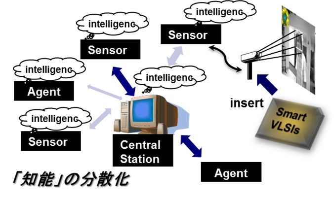
In such a system, both of learning and recognition (for instance) are carried out at the edge instead of central stations, which is helpful to reduce the communications and able to active movable equipment off-connecting any PC (such as vehicles and body-area). Unfortunately, very few on-chip learning processors have been developed for machine learning at edge in silicon.
Both of digital and analog efforts have been done a lot to develop on-chip learning processors. Multi-computational-core is a general digital strategy to process a large number of complex computations in parallel (see machine learning works by GPGPU). Our group members also hold some experiences of implementing machine learning by CGRAs with very high parallelism. For many IoT tasks, the computational accuracy is not extremely required. Therefore, some approximate computing processors were designed by analog circuits. In some of my early works, it is found the chaos of analog signals greatly speeds up the learning process. We have realized ultra-high speed on-chip learning for some specific algorithms such as SVM or K-means. In summary, the CPU or GPGPU is not always applicable for every edge device; analog processors have potentials of high-speed and low-power, but their functions (target algorithms) are always fixed and specific. Therefore, most of current/previous IoT works, which employ machine learning, have to carry out the “learning” centrally, then do the recognitions locally.
What have we done?
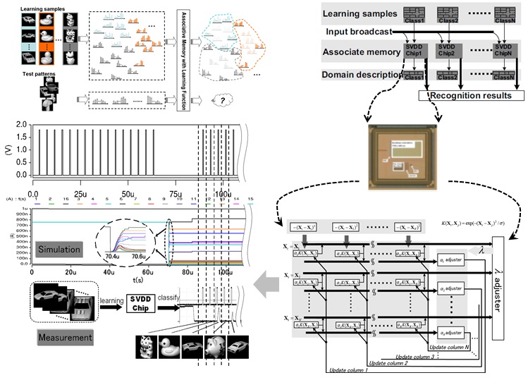
On the academia side, the ML and AI research/development is one of the most popular fields. There are many groups and societies are trying to design specific VLSI systems for realizing efficient ML. Most of those works are based on the high performance digital processors. The analog (even physics device) circuit has been a new (or we can say re-born) trend leading to ultra-high speed and efficiency. Our early work was one of world-first pure-analog ML chips with benefits but suffered from poor generalization. Thus, we are going to develop generally and practically feasible technologies in this field. In industry, many software/hardware makers start their competitions on VLSI chips for ML/AI in past five years (see “IBM Scientists Show Blueprints for Brain-like Computing,” “Building a Brain on a Silicon Chip” and “Intel Reveals Neuromorphic Chip Design”). The mobile supplier HUAWEI even actually applied the NPU (Neural Processing Unit) in their newest mobile chip “Kirin970”. In our early works, world fastest learning (64-D SVM learning within 0.1us, 2012; 64-D K-means within 20ns, 2013; 64-D SVDD within 40ns, 2014) has been achieved (see the sided figure as an example: SVDD algorithm is implemented by VLSI to do the multi-class image classification). However, the algorithms and capacities were fixed. We expect to keep the speed benefit and generalize the target algorithms.
What are we going to do?
As an exploration, we are expecting to develop general purpose on-chip learning processor which accelerates various machine learning processes by analog VLSIs. As consequence, local/on-chip machine learning is feasible and practical for ubiquitous applications.
We are designing ultra-high speed and low-energy hardware (VLSIs) for implementing the so-called on-chip learning (not for specific but various algorithms). The analog approximate computing strategy is adapted. The circuit-, unit-, and architecture-level are explored; several actual VLSI chips are expected to fabricate as demonstrations. For instance, we will demo the visual tracking with ML by a single VLSI chip without any PC.
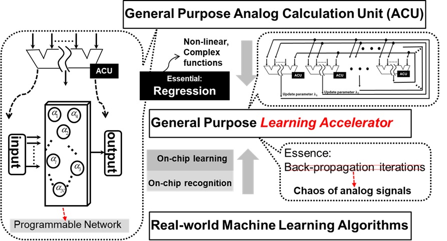
As shown in the sided figure, three key ideas are included in this project: 1. General purpose Analog Calculation Unit (called ACU); 2. Fully-parallel accelerating strategy; 3. Expanding the learning capacity. It is a cross-field among high-performance-computing, the VLSI designs and machine learning theories.
What are we expecting?
Firstly, we expect our novel learning mode: chaos of continuous signals, to impact the machine learning societies for reasonable applications. Along with the development of IoT, various demands of on-chip machine learning require the well-performance hardware besides CPU or GPGPU. Secondly, a general purpose ML accelerator leads to practical “smart chips”, which are embedded into the edge-devices of IoT. Currently, most of IoT works execute the recognition at the edge, but do the learning process on cloud or central stations. The edge learning offers a potential for industry to build more efficient and intelligent network, in which the machine learning can be done by VLSI chips instead of CPUs.
Most importantly, the road-map of VLSI scaling-down might reach the end soon. Different strategies of high performance computing architecture should be explored. The progress of this project is expected to push the analog approximate computing fashion into practical fields. The developed ACUs can be applied in various architectures even together with digital frameworks. The general purpose and programmable analog computing, as an internal progress, offers a different option of data processing: lighter, but faster.
Thank you very much for your kind reading.