Secure the Internet of Things (IoT) using Physical Layer Security and Blockchain

Hi, everyone! This is Yuanyu Zhang from the Large-Scale Systems Management Laboratory.  It is a great opportunity for me to share my research with you. Broadly speaking, my research focuses on the security of Internet of Things (IoT) systems, with special interests in securing IoT wireless communications based on physical layer security (PLS) technology and designing access control schemes based on the emerging blockchain technology. Now, I am going to briefly introduce my research from these two aspects.

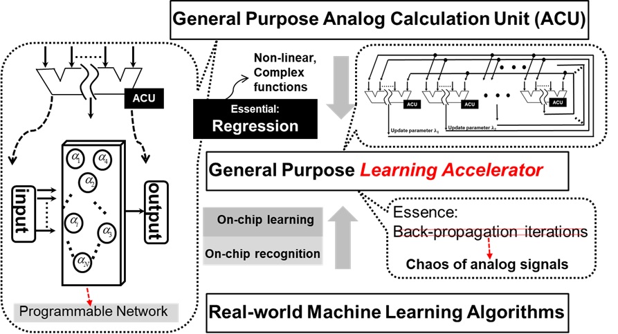
  • PLS-based Secure IoT Wireless Communications 

When it comes to the IoT, I believe anyone can give an concrete application, such as smart home, e-health, intelligent transportation, etc. In these applications, a huge number of smart devices, like sensors, actuators, tablets, will be connected into the Internet via a variety of wireless communication technologies, like WiFi, Zigbee and Bluetooth.  As we all know, wireless medium is open such that anyone close to a transmitter can receive its signals. Suppose the information conveyed by the signal is not encrypted, so what would happen if the signal is received by an eavesdropper? Obviously, the information is in danger! In IoT applications, these information may be your health data perceived by sensors around you and your financial transfer records sent from smart phones. Once these information are leaked to eavesdroppers, your life and property will be in danger.

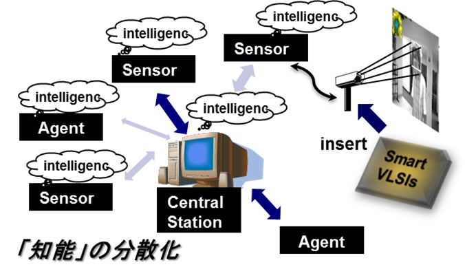
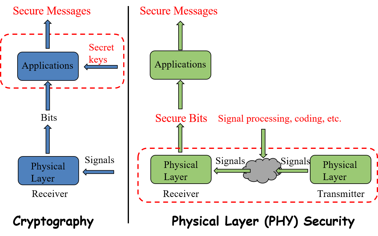
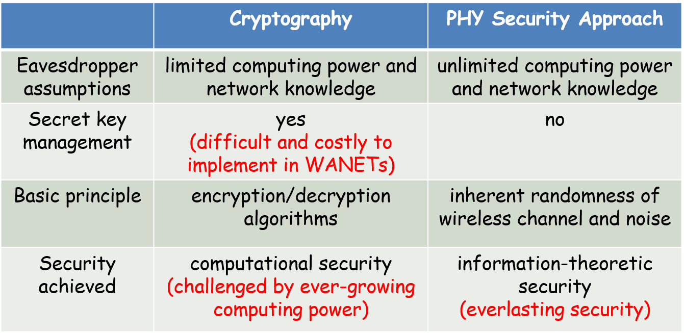
Of course, we can encrypt these information using secret key-based cryptographic approaches like what we do in wired communications. However, managing and distributing secret keys in wireless environment is challenging, especially for large-scale IoT systems. Besides, the cryptographic approaches usually require high computing power, which is unavailable for most resource-constrained IoT devices. This motivates the advent of the so-called physical layer security (PLS) technology, which uses the inherent randomness of wireless channels (e.g., fading, noise, interference) instead of costly cryptographic approaches to ensure no information leaked to eavesdroppers. As long as we can guarantee that the received signal of the eavesdropper is an degraded version of that of the intended receiver, the eavesdropper can abstract nothing from the signal. This conclusion has been proved from the perspective of information theory. The figures below shows the basic differences between cryptographic approaches and PLS technology.

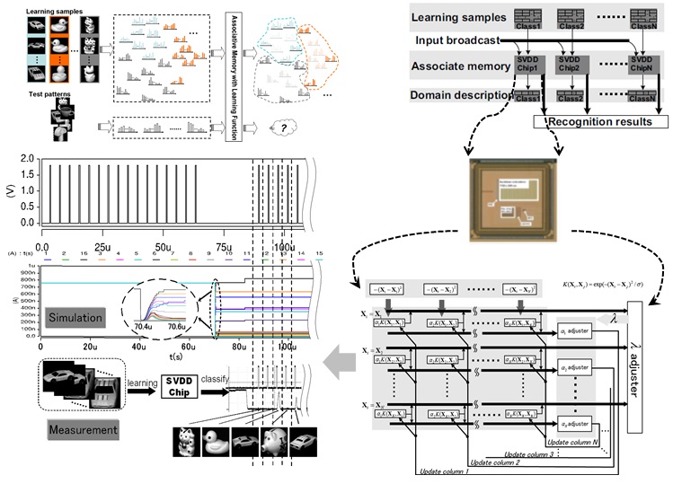
What my research does is to apply commonly-used PLS techniques in IoT systems and theoretically evaluate the security performances of these systems using some mathematical tools, like Probability Theory, Markov Chain Theory, Queuing Theory and Stochastic Geometry.  Well, okay, I know it’s boring, but trust me, it is vitally important for understanding the PLS performance limits of IoT systems and contributing to the successful application of PLS techniques in these systems. If it does not sound boring to you, I would be very glad to share this research with you in greater details.

  • Blockchain-based IoT Access Control

Okay, ready for another research? You know what, this research may be more interesting, at least for me. The previous research focuses on the security of the information during its transmission, while this research focuses on the security of the information when it is stored somewhere as resource and accessed by some users or devices. Of course, resources are not limited to information, but also include actuators that may perform some critical tasks, like brake control and drug delivery.  But one common thing is that, once these resources are accessed by malicious users, your life and property will be in danger. This research aims to design effective access control schemes to prevent illegal access to IoT resources.

Traditional access control schemes are centralized, which means that they use a central server to control all access requests in the system. So what if this server is destroyed in disasters, or what if this server is compromised by some malicious guy? Yes, the whole access control scheme collapses.  Now, question is how to tackle these challenging issues. Fortunately, the emerging blockchain technology provides us with a promising solution, because it is highly distributed and ensures reliable financial transactions among trustless peers all over the world. In this research, I use the Ethereum blockchain, which evolves into a distributed and reliable computing platform thanks to the introduction of smart contract. A smart contract can be thought of as a piece of code that is stored on the blockchain and distributed to all nodes in the system. All nodes can execute this code and verify the correctness of the results. This ensures the correct execution of the smart contract as long as no one possesses more than 51% of the system computing power.

The basic idea of this research is to ensure  distributed and reliable access control by expressing the access control policies and logic as smart contracts. The access control framework is illustrated in the figure below.

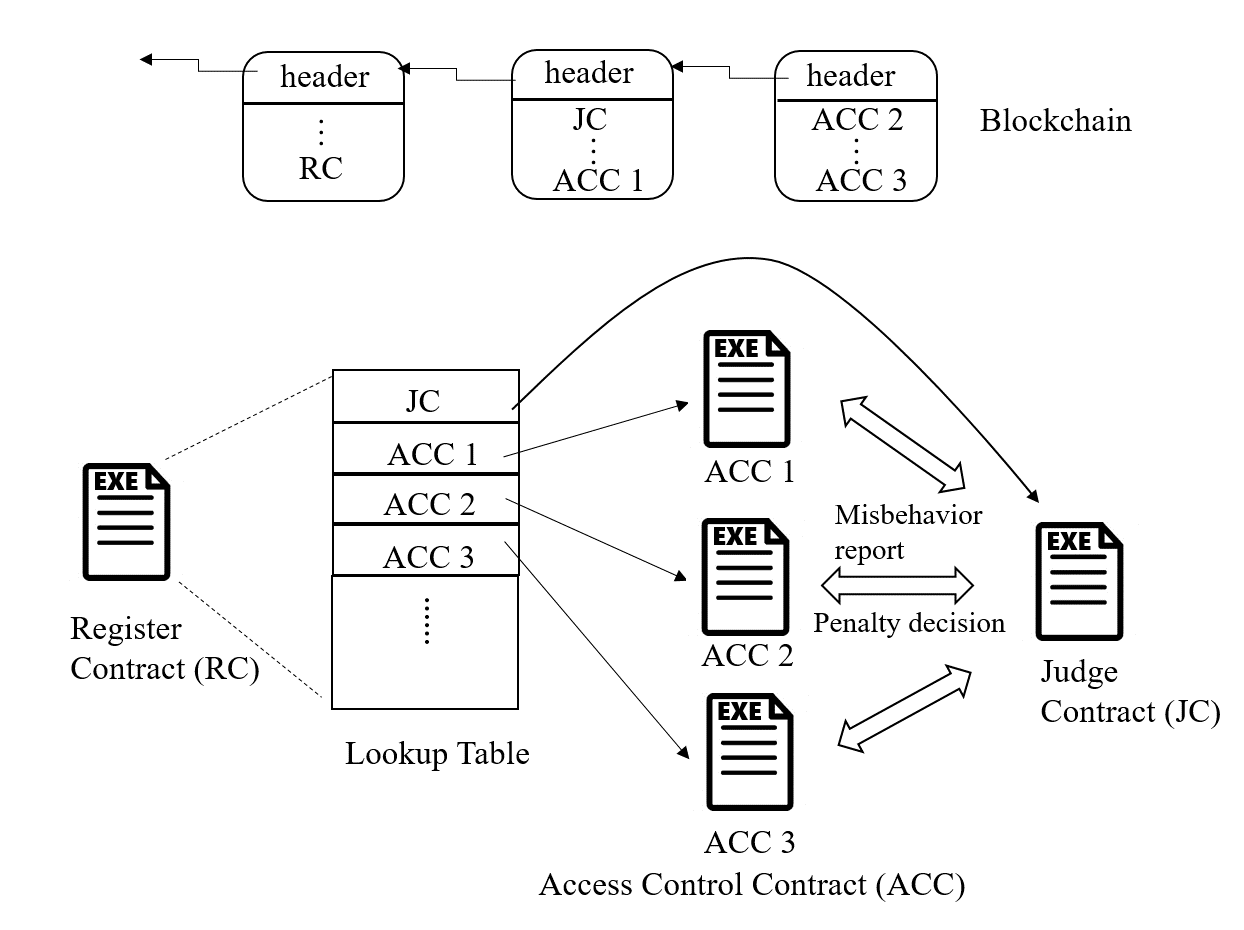
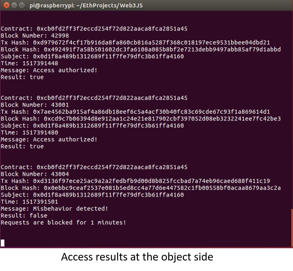
This framework consists of multiple access control contracts (ACCs), one judge contract (JC) and one register contract (RC). Each ACC is responsible for the access control of a subject-object pair, and implements both static access right validation based on predefined policies and dynamic access right validation by checking the behavior of the subject. Here, a subject is the node accessing the resources possessed by an object. The JC implements the misbehavior-judging method to facilitate the dynamic validation of the ACCs by receiving misbehavior reports from the ACCs, judging the misbehavior and returning the corresponding penalty. The RC registers the information of ACCs and JC, and also provides functions (e.g., register, update and delete) to manage these methods. Suppose a server wants to access the resource of a camera in a smart home. The workflow of the access control is shown in the figure below.

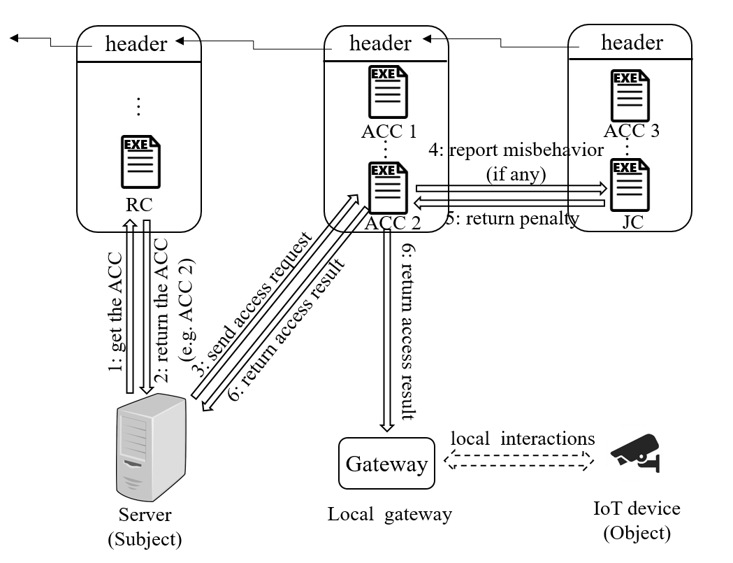
  • Step 1: The server calls the RC to retrieve the ACC (e.g., the ACC 2) for access control.
  • Step 2: The RC returns the address and ABI (similar to API) of the ACC to the server.
  • Step 3: The server sends a transaction to the ACC, which contains the required information for access control. This transaction will be encapsulated in a new block and the ACC will not be executed until the new block is mined and included in the blockchain by some miner.
  • Step 4: During the access control process, the ACC will send a message to call the JC, if some potential misbehavior of the subject is detected.
  • Step 5: Once the JC  judges the misbehavior and determines the penalty, it will return the penalty to the ACC.
  • Step 6: Finally, the access result will be returned to both the subject and object, after the access control process finishes.

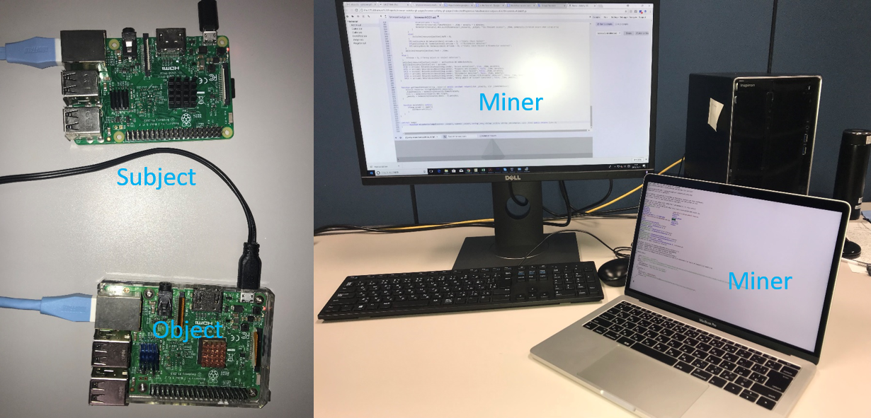
To demonstrate the feasibility of the framework, we provide a case study in an IoT system with one desktop computer, one laptop and two Raspberry Pi single-board computers, as shown in the figure below.

And the results of access control at both the subject and object sides are illustrated in the figures below.

光メディアインタフェース研究室 2018

光メディアインタフェース研究室 助教の田中です.前回の投稿は,2015年3月「光メディアインタフェース研究室 本格始動!」でした.あの時は,研究室が発足したばっかりでしたが,いまや学生はM1からD3まで勢揃いの立派な研究室になりました.今回は,これまでの本研究室の成果を振り返ってみます.

光メディアインタフェース研究室は,1.機械がカメラを通して現実を理解する「コンピュータビジョン」 2.あらゆる物体の質感をリアルに再現する「コンピュータグラフィクス」 3.カメラの常識を打ち破る新しい撮影技術「コンピューテーショナルフォトグラフィ」 4.あらゆる研究の基礎となる「光学設計」の4本柱で研究を進めており,人間と機械が光を媒体としてシーンに関する情報を共有できる新しいインタフェースの実現を目指し活動しています.詳しい研究内容は,研究室ホームページ  をご参照ください.


今,光メディアインタフェース研究室には,教授・准教授・2名の助教の計4名の教員,事務補佐員,6名の博士後期課程学生,16名の博士前期課程学生,さらに1名のインターン生で活動しています.研究室の学生は,毎年何らかの研究予算を自分で獲得してきてプロジェクトを進めるなど,活発な人が多く在籍しています.CICPと呼ばれる学内予算はもとより,日本学術振興会特別研究員や,JST ACT-I,IPA未踏スーパークリエーター認定などを得ており,自ら未開拓分野を切り拓いていく姿勢には感心します.これまでに,本研究室を修了した学生は,3年間で延べ21人となり,各方面で活躍しています.「光メディアインタフェース研究室出身はすごい」と呼ばれるよう,より一層の活躍を期待したいところです.また,これまで多数の留学生・インターン等を受け入れています.なぜだか分かりませんが,多くがフランス語圏からの留学生です.もしかして,フランス語の案内ページも作ったほうが良いのでしょうか…?

本研究室は,活発に外部の機関と共同研究を実施してきました.複数の国内大手電機メーカーや農業・医療・自動車産業,アニメ産業の企業と連携中あるいは連携してきました.アカデミックでは,東京大学・京都大学・大阪大学・九州大学・国立情報学研究所・筑波大学・広島大学・早稲田大学・東邦大学や,Carnegie Mellon University (CMU・アメリカ)・Arizona State University(アメリカ)・The University of Picardie Joule Verne (フランス)・The University of California Los Angeles (UCLA・アメリカ) の研究者と共同研究を実施してきました.プロジェクトの数が多く,学生が多数の幅広いテーマから自分のやりたいことを選択し取り組めるのも,この研究室の大きな特徴かもしれません.

彼らとともに成し遂げた研究プロジェクトは http://omilab.naist.jp/publications-jp.html から見ることができます.数字で見ていくと,情報電子通信学会論文賞やMIRU長尾賞などの大きな賞を含む24個の受賞,2本のPAMI(最難関国際論文誌)を含む12本の論文誌および5本のCVPR(最難関国際会議)を含む21本の査読付き国際会議論文を発表してきました.どのテーマで研究しても,在学中に1回以上の発表を学会で行うべく,ハイレベルな研究活動を行っています.


ここで,大きな賞を受賞した2つの研究を少し紹介したいと思います.一つ目は,電子情報通信学会論文賞やMIRUフロンティア賞を受賞している,一連の新しいコンピュータグラフィクス(CG)の研究です.多くの人は,CGと聞くと,ゲームや映画で使われているようなきれいな画を作る技術だと思われているでしょう.これまでのCG技術の一つに,現実の物体を計測し,それそっくりな見た目の映像を計測データを使って「画面上で」リアルに表現するというものがありました.我々の研究室では,この「画面上」という制限を取っ払って,「リアル空間で」計測した物体そっくりのレプリカをつくろうという新しい表現方法を研究しています.つまり,物体の形状と質感を,3Dプリンタや高度な印刷技術,微細構造の工夫などによって,現実空間にコピーする技術の開発を行っています.図1にこの研究の例を示しています.この実験では,計測したサーモンの質感を,ロウでできた物体にコピーしています.写真ではわかりにくいかもしれませんが,どこからみてもサーモンっぽい質感の再現に成功しました.この技術が発展すれば,本物の美術品や古典籍にそっくりな触れるレプリカの作成,個人個人の肌とそっくりな義手・義足や,エンターテインメントなど,コンピュータグラフィクス技術の新しい社会実装に貢献できるのではないかと考えています.


図1:本物のサーモン(左)とリアルな見た目のレプリカ(右)


2つ目の研究は,MIRU長尾賞という,いわゆる日本一と認められた,新しいコンピュータビジョンの研究です.コンピュータビジョンというと,カメラで撮影された視覚情報をコンピュータでどのように理解するか,という風に説明されてきました.我々の研究室では,カメラで撮影された後の2次元画像からスタートしているようでは情報が不十分であり,画像になる前の,現実世界を飛び交う光の状態からシーン理解を行うべきだという信念のもと,より次元を増やした計測からシーン理解を行う研究を行っています.その中でも,時間の次元を増やす,ということに関して,世界のトップレベルとしのぎを削っています.時間の次元と言っても,単にビデオやハイスピードカメラで撮影するということではありません.この研究室で行っているのは,「光」自体が伝わっていく様子を可視化できるくらいの超高速な計測,時間で言うと数ナノ秒(0.000000001秒)から数ピコ秒(0.000000000001秒)です.図2に,実際に 250ピコ秒で撮影した画像を載せています.このレベルになると,光がどのように反射・散乱し,シーン中を伝わっていくのかが分かります.当然ながら,こうした情報を使うと,3次元形状,物体の材質,異常検知などが簡単に行えるようになります.

 
図2:シーン(左)中を光が伝播していく様子(右)

光メディアインタフェース研究室では,現在,向川教授を研究代表とした大型プロジェクト「多元光情報の符号化計測と高次元化処理の協調設計」を実施しています.このプロジェクトでは,計測の次元を「時間」だけでなく,「波長」や「空間」といった次元にも拡張していき,高度な計測技術を確立することを目指しています.博士課程やポスドクとして参画したい方,コンタクトください.


最後に,NAISTへの入学を検討している方や,インターン希望の方,ぜひ一度光メディアインタフェース研究室に見学に来てください.文章ではわからない研究のこと,研究室の雰囲気,研究の進め方,などなど,今後の進路に役立つこと間違いありません.NAISTでは,受験生のためのオープンキャンパス を毎年2月と5月に行っています.また,受験を検討している人のために2・3日の研究体験ができるサマーセミナー (8月頃)や スプリングセミナー (2月頃)もやっています.さらに,いつでも見学会 という制度を使うと,研究室が受け入れ可能な日はいつでも見学・相談が可能です.ぜひ,ご検討ください.

Speed Up Machine Learning Through Efforts of Advanced VLSI Circuits

Hello, world. This is from Assistant Professor Renyuan Zhang with Computing Architecture Lab. to share some progresses from our group, which are all about speeding up the machine learnings through efforts of advanced VLSI circuits.

Why do we implement the machine learning in silicon?

The artificial intelligence plays very important roles in the modern/post IoT. A common challenge is how to efficiently implement machine learning algorithms in systems with the cloud-edge prototype. Along with the development of computing processors, one option is to distribute the machine learning at the “edge” of systems as show in the sided figure.

In such a system, both of learning and recognition (for instance) are carried out at the edge instead of central stations, which is helpful to reduce the communications and able to active movable equipment off-connecting any PC (such as vehicles and body-area). Unfortunately, very few on-chip learning processors have been developed for machine learning at edge in silicon.

Both of digital and analog efforts have been done a lot to develop on-chip learning processors. Multi-computational-core is a general digital strategy to process a large number of complex computations in parallel (see machine learning works by GPGPU). Our group members also hold some experiences of implementing machine learning by CGRAs with very high parallelism. For many IoT tasks, the computational accuracy is not extremely required. Therefore, some approximate computing processors were designed by analog circuits. In some of my early works, it is found the chaos of analog signals greatly speeds up the learning process. We have realized ultra-high speed on-chip learning for some specific algorithms such as SVM or K-means. In summary, the CPU or GPGPU is not always applicable for every edge device; analog processors have potentials of high-speed and low-power, but their functions (target algorithms) are always fixed and specific. Therefore, most of current/previous IoT works, which employ machine learning, have to carry out the “learning” centrally, then do the recognitions locally.

What have we done?

On the academia side, the ML and AI research/development is one of the most popular fields. There are many groups and societies are trying to design specific VLSI systems for realizing efficient ML. Most of those works are based on the high performance digital processors. The analog (even physics device) circuit has been a new (or we can say re-born) trend leading to ultra-high speed and efficiency. Our early work was one of world-first pure-analog ML chips with benefits but suffered from poor generalization. Thus, we are going to develop generally and practically feasible technologies in this field. In industry, many software/hardware makers start their competitions on VLSI chips for ML/AI in past five years (see “IBM Scientists Show Blueprints for Brain-like Computing,” “Building a Brain on a Silicon Chip” and “Intel Reveals Neuromorphic Chip Design”). The mobile supplier HUAWEI even actually applied the NPU (Neural Processing Unit) in their newest mobile chip “Kirin970”.  In our early works, world fastest learning (64-D SVM learning within 0.1us, 2012; 64-D K-means within 20ns, 2013; 64-D SVDD within 40ns, 2014) has been achieved (see the sided figure as an example: SVDD algorithm is implemented by VLSI to do the multi-class image classification). However, the algorithms and capacities were fixed. We expect to keep the speed benefit and generalize the target algorithms.

What are we going to do?

As an exploration, we are expecting to develop general purpose on-chip learning processor which accelerates various machine learning processes by analog VLSIs. As consequence, local/on-chip machine learning is feasible and practical for ubiquitous applications.

We are designing ultra-high speed and low-energy hardware (VLSIs) for implementing the so-called on-chip learning (not for specific but various algorithms). The analog approximate computing strategy is adapted. The circuit-, unit-, and architecture-level are explored; several actual VLSI chips are expected to fabricate as demonstrations. For instance, we will demo the visual tracking with ML by a single VLSI chip without any PC.

As shown in the sided figure, three key ideas are included in this project: 1. General purpose Analog Calculation Unit (called ACU); 2. Fully-parallel accelerating strategy; 3. Expanding the learning capacity. It is a cross-field among high-performance-computing, the VLSI designs and machine learning theories.

What are we expecting?

Firstly, we expect our novel learning mode: chaos of continuous signals, to impact the machine learning societies for reasonable applications. Along with the development of IoT, various demands of on-chip machine learning require the well-performance hardware besides CPU or GPGPU. Secondly, a general purpose ML accelerator leads to practical “smart chips”, which are embedded into the edge-devices of IoT. Currently, most of IoT works execute the recognition at the edge, but do the learning process on cloud or central stations. The edge learning offers a potential for industry to build more efficient and intelligent network, in which the machine learning can be done by VLSI chips instead of CPUs.

Most importantly, the road-map of VLSI scaling-down might reach the end soon. Different strategies of high performance computing architecture should be explored. The progress of this project is expected to push the analog approximate computing fashion into practical fields. The developed ACUs can be applied in various architectures even together with digital frameworks. The general purpose and programmable analog computing, as an internal progress, offers a different option of data processing: lighter, but faster.

Thank you very much for your kind reading.

電力変換回路の高効率開発に向けた電熱連成解析

ディペンダブルシステム学研究室助教の新谷です。今日は、我々の研究テーマの1つであるパワーMOSFETのモデル化に関する研究を紹介いたします。

パワーMOSFETと発熱
現在、世界各国で電気自動車の開発が盛んに進められています。電気自動車のモーター出力は120kW以上が要求され、そのためには、電源電圧600Vであれば電流200A以上となります。このような、大電流、大電圧の環境下で使用されるパワーMOSFETの性能は、耐圧1200V以上、100A以上を扱えることが最低条件になります。

このような大電力を扱う回路において、最も重要な設計制約は「熱」です。パワーMOSFETはスイッチング時にスイッチング損失を生じます。ドレイン端子からソース端子に流れる電流に生じる導通損失、ゲート端子に寄生する容量成分で生じるゲート電荷損失などがあり、PCやスマートフォンなどに搭載されるマイクロデバイスとは比べ物にならないほど高い値になります。これらの電力損失は熱として現れ、回路特性およびパワーMOSFET周辺に設置された素子に大きな影響を与えます。したがって、高い信頼性が要求される電力変換回路の設計では、設計早期段階でホットスポット(発熱が大きい箇所)を知り、これを考慮した熱設計が必須といえます。従来は、電気特性は回路シミュレーションを行い、熱特性については電磁界解析シミュレータにより行う、というように電気特性と熱特性を分けて解析する手法が主流であり、同時に解析することは困難とされてきました。

そこで、熱特性と電気特性に類似性があり熱特性においても電気特性の基礎法則であるオームの法則が成り立つことに着目しました。表1のように、熱流量、温度はそれぞれ電流、電圧、電位差に置き換えられることができます。抵抗などはそのまま、熱の伝わりにくさを示す熱抵抗となります。我々の研究グループでは、熱特性を電気回路で模した熱回路を用いることで、回路シミュレーション上で電気特性と熱特性を同時に解析する連成解析手法を可能にしました。

表1: 電気特性と熱特性の類似性

電気特性 温度特性
電圧 (V) 温度 (°C)
抵抗 (Ω) 熱抵抗 (°C/W)
容量 (F) 熱容量 (J/°Cm3)
電流 (A) 熱量 (J)
消費電力 (W) 熱流量 (J/s)


電熱回路シミュレーションモデル
電熱連成解析実現のために、図1に示すような回路シミュレーションモデルを構築しました。本モデルでは、電気特性と熱特性が相互に依存し合うようになっています。まず、図1の左部分は、パワーMOSFETの電気特性であり、与えられた温度、電圧条件における電流値を計算します。電圧と計算した電流から、MOSFETで消費される電力が計算可能となります。図2の右側は熱回路になります。MOSFETモデルで計算した消費電力を入力とし、デバイスの発熱温度が計算されます。表1から、電気特性で計算された消費電力は、熱特性モデルにおける熱流量のように扱うことができます。熱回路は、一般的に熱抵抗と熱容量から構成されます。ここでは、フォスター回路型と呼ばれる多段RC回路を採用しました。このRC回路により、MOSFETを包むパッケージ樹脂における熱の通しやすさをモデル化しています。熱回路で計算された温度は、再度MOSFETモデルに戻され、この温度および電圧条件での電流を計算します。これらの計算処理は、全て回路シミュレータで行われます。既存の方法では、2つのシミュレータにまたがって行われていた計算を一度に行うことができます。


図1: 電気特性モデルと熱特性モデル

さて、図1のモデルを用いて、任意のデバイスの特性を表現できるようにするためには、モデルのパラメータをデバイスに合わせる必要があります。具体的には、次の2つの手順が必要です。

  1. 温度を考慮した電気特性モデルパラメータの推定
  2. 熱特性モデルパラメータの推定


温度を考慮した電気特性モデルパラメータの推定
まず、電気特性モデルで使用されるパラメータを抽出します。電気特性モデルは、その特性を正確に再現するために、いくつかのパラメータで構成されています。MOSFETモデルの場合、フラットバンド電圧、寄生抵抗成分、移動度があります。電気特性モデルを用いることで、電流の特性を計算することができますが、電流が多く流れるデバイスもあれば、電流量が少ないデバイスもあります。そこで、モデル化対象となるデバイスの実測結果をよく再現するようにパラメータを最適化・抽出する必要があり、この工程をパラメータ抽出と呼びます。

ここでは、図2に示すように、温度毎に電流特性とシミュレーションモデルを一致させました。上述のフラットバンド電圧、移動度などのパラメータは、温度に対して一次の依存性を持つことが知られているため、パラメータを温度の1次関数とみなして抽出を行っています。このように、モデルパラメータに温度依存性を持たせることで、図2のように任意の温度における電流値を計算することができます。


図2: 温度毎の電流特性とそのモデル。点が電流の実測値で、線がシミュレーションによる計算結果を表す。


熱特性モデルパラメータの推定
上述のように、熱特性モデルは抵抗と容量から構成される多段RC回路でモデル化されています。これらの抵抗値、容量値はどのように求めれば良いのでしょうか。図1のシミュレーションモデルは、図3に示すようなフィードバック制御回路として表現できます。我々は、この熱特性モデルを熱伝達特性とみなして、熱特性モデルのパラメータ推定手法を開発しました。


図3: フィードバック制御図

具体的には、図4のように、パルス幅変調(PWM)機構を用いてMOSFETに対する電力を一定に保ちながら、チップの熱応答を測定する手法を提案しました。PWM機構を用いて、一定周期で現在の電力を計算し、電力を一定に保つように電流の導通時間を制御することで常に平均消費電力が一定になるよう制御します。これにより、伝達関数のステップ応答を直接測定可能になり、複雑な数値処理を行うことなくパラメータを求めることが可能になります。


図4: パルス幅変調回路による電力保持機構


バックコンバータを用いた評価
最後に、代表的な電力変換回路であるバックコンバータを用いた評価結果を示します。バックコンバータの回路図は図5の左図で示され、SiCショットキーバリアダイオード(SBD)とSiCパワーMOSFETを含みます。実際に作成した回路は図5の右図になります。この評価では、実測した電気特性と熱特性の過渡的な変化と回路シミュレーション結果による比較を行いました。回路シミュレーションは、市販のSPICE回路シミュレータに、開発した電気特性モデルおよび熱特性モデルを組み込むことで行っています。


図5: バックコンバータの回路図とプリント基板への実装

図6に電気特性および熱特性の過渡解析結果を示します。まず、電気特性、熱特性ともに実測結果とシミュレーションともに非常によく合っていることがわかります。特に、熱解析においては600秒までの過渡的な変化を正確に模擬しており、その誤差は7.52%以下、と非常に高精度なものとなっております。


図6: 電気特性(左)と熱特性(右)の過渡変化の実測とシミュレーションの比較


終わりに
以上が、これまでの研究成果の一部の紹介です。地球資源に依存しないクリーンなエネルギーは全世界が注目する研究分野であり、本研究はその一端を担ったものです。近年のパワーエレクトロニクスの進展はすさまじいものがあり、本研究の成果によりパワーエレクトロニクス企業からお声がけいただくことも多く、科学技術振興機構の産学共創プラットフォーム共同研究推進プログラム(OPERA)に一研究グループとして参加しています。最近では、電力変換回路の最適化に関して機械学習を応用した手法の研究にも取り組んでおり、情報科学と電気電子工学の両方を学びたい学生にはちょうど良い研究テーマです。また、計算機上のプログラムによる確認にとどまらず,自ら考えた回路を試作して動作を確認するため、アイデアを具現化する達成感を味わうことができます。


生物に倣うロボットの制御

こんにちは,知能システム制御研究室助教の小林です.

ロボットというのは往々にして生物を手本にその機構や制御を設計します.何故なら,生物というのはその誕生から進化をし続けて現在の環境へと最適化されているからです.そんな生物の機構や制御を紐解けば,ロボットにとっても最適な機構や制御を導くことができます.例えば私の過去の研究では,ヒューマノイドロボットの歩行制御を人の歩行の特徴,モデルを基に設計することで人のような省エネな歩行を実現してきました.最近では,生物の運動制御を司る小脳の神経回路網を模倣したReservoir Computingを利用した継続学習に挑戦しています.
なお,研究室の詳しい情報は研究室HPを,私のその他の研究については個人HPをご覧ください.

これまでの研究

この歩行に関する研究は「マルチロコモーションロボット」というプロジェクトの一環で行ってきました.マルチロコモーションロボットというのは,ロボットが単一の移動形態,例えば2足歩行,だけを利用して環境に適応しようとするのではなく,複数の移動形態から最適なものを直面している状況に応じて適宜選択・切り替えていくことでより複雑な環境に適応する,というコンセプトです.これもやはり生物に倣っていて,人を例に見れば,普段は歩きますが急ぐ時は走りますし,梯子を登ったり,山道では両手にトレッキングポールという杖を持って脚への負担の分散,つまり4足歩行をするはずです.この複数の移動形態というのは,それぞれが得意な環境・苦手な環境がありますので,互いの短所を補い合い長所だけを上手く利用すれば,単一の移動形態だけを駆使するよりも遥かに優れた環境適応能力を得られます.

では,そんな複数の移動形態を扱うにはどうすれば良いのでしょうか?単純に考えれば,各移動形態を実現する制御器を別々に用意すれば良いと思うでしょう.しかしこの移動形態というのは細かく分ければ無数に存在しますので,全てを別の制御器で扱うというのは現実的ではありません.そのため,複数の移動形態を可能な限り統一的に扱うような制御器を設計することが求められます.そんな制御器として,環境との受動的な点接触と全身関節角が接触角に連動して動く仮想拘束の2つの原理を組み込んだPassive Dynamic Autonomous Control (PDAC)という手法を提案してきました.この2つはロボットの全身ダイナミクスを非常に簡単なものにしてくれ,さらには,環境と何処で接触しているのか,どのように連動させるか,の2点だけを考えれば全ての移動形態を制御できるようにしてくれます.

特に連動のルール,すなわち仮想拘束を上手に与えると,似た移動形態をさらに統一的に扱うことができます.2足歩行と走行を例に見れば,両脚が地面から離れる跳躍期の有無という違いはあるものの,その本質は左右の脚を交互に振り出していくという共通点があります.人の歩行と走行の解析をして得られたモデルも倒立振子を基にしており,振子の剛性(歩行では硬く,走行では柔らかい)という差異はあるものの,十分に共通化できるものとなっています.この共通化されたモデルに従って仮想拘束を与えると,ただ歩行と走行を扱えるだけでなく,両者間を共通化されたモデルのパラメータ1つを変えるだけで容易に切り替えることが可能になります.ちなみに,この切り替えタイミングについても生物の特徴を取り入れることができます.生物が歩行と走行を切り替えるのは,移動距離当たりのエネルギー消費を最小化するためということが解明されています.つまり,ロボットでも歩行と走行のエネルギー消費を比較して関係が逆転するタイミングで切り替えれば良いのです.
このように生物の特徴をふんだんに取り入れて設計された制御器は,生物のように低速時には歩行を,高速時には走行を自然と実行することができます.

最近の研究

生物の何処が身体を上手に制御しているかと言えば,それは間違いなく脳だと言えるでしょう.つまり,生物の脳構造を紐解いて模倣することができれば,生物のように巧みな動きが実現できるはずです.脳構造を模倣したもの全般はニューラルネットワークと呼ばれ,最近ではこのネットワークの層構造を何十,何百層とした,いわゆる深層学習が認識技術として大きな成功を収めています.この深層学習は人の視覚野と似た情報処理構造をしているとされていますが,では運動制御を司っている小脳を模倣した情報処理構造はどうなっているのでしょうか?その答えがLiquid State Machine (LSM)やEcho State Network (ESN)に代表されるReservoir Computingになります.

Reservoir Computingは入力層・リザーバ層・出力層の3層で構成され,このリザーバ層が自身の信号を再び取り入れるという,再帰的な結合を持つリカレントニューラルネットワークの一種となります.Reservoir Computingの最たる特徴は,学習するノード間の結合がリザーバ層と出力層を接続しているリードアウトのみ,という点にあります.つまり,一般的なニューラルネットワークと異なり,出力層における誤差を逆伝播させることなく,リザーバ層は初期のランダムな結合のままで固有のダイナミクスを有したままとなります.このリザーバ層の構造が小脳における顆粒層に相当するといわれています.また,リザーバ層を学習しないで良いため,そのノード数は通常のニューラルネットワークより非常に大きくしやすくなっており(1千〜1万個など),顆粒層(1000億個ほど)と比べればまだまだ少ないですが,それでも類似した特徴といえます.

最近は,このReservoir Computingを用いた継続学習について研究しています.一般的なニューラルネットワークというのは,誤差逆伝播によってネットワーク全体の結合荷重を更新して学習したいタスクを獲得するため,タスクAについて学習済みのネットワークでタスクBを学習すると,タスクAを扱えなくなる「破滅的忘却」という問題を抱えています.Reservoir Computingであれば,リードアウトをスパースに学習するだけでタスク間の競合を最小限に抑えられます.また,リザーバ層にあるタスク入力を加えれば,固有のダイナミクスに基づいた入力依存の活性化パターンが期待されますので,タスクごとに異なるノードが活性化しやすいようになります.こういった工夫を取り入れることで従来のように全てのタスクについて同時に学習するのではなく,生物のようにタスクを1つずつ継続的に学習することができます.この継続学習は,生物のように生涯を通じて学習し続けて次々に新しいことができるようになる自律ロボットを開発するにあたって非常に重要な能力になります.